Home
/ Fermi Level In Semiconductor : Quasi Fermi Levels Explained Youtube / Here ef is called the.
Fermi Level In Semiconductor : Quasi Fermi Levels Explained Youtube / Here ef is called the.
Fermi Level In Semiconductor : Quasi Fermi Levels Explained Youtube / Here ef is called the.. The fermi level does not include the work required to remove the electron from wherever it came from. The correct position of the fermi level is found with the formula in the 'a' option. The fermi level determines the probability of electron occupancy at different energy levels. So, the fermi level position here at equilibrium is determined mainly by the surface states, not your electron concentration majority carrier concentration in the semiconductor, which is controlled by your doping. Uniform electric field on uniform sample 2.
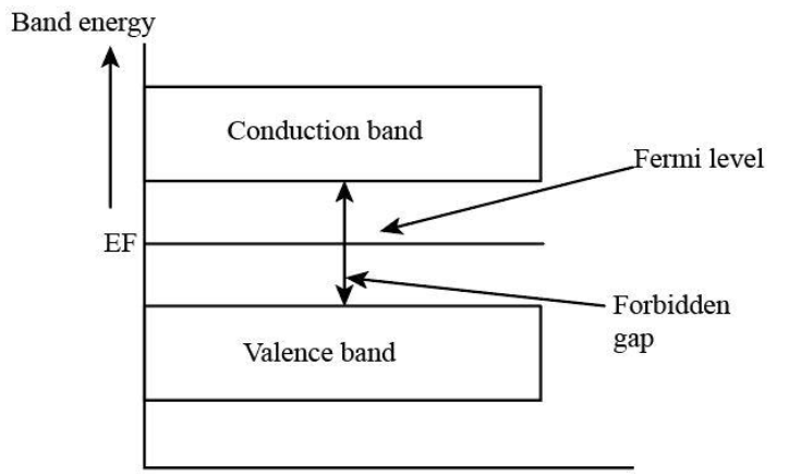
As a result, they are characterized by an equal chance of finding a hole as that of an electron. If so, give us a like in the sidebar. We mentioned earlier that the fermi level lies within the forbidden gap, which basically results from the need to maintain equal concentrations of electrons and (15) and (16) be equal at all temperatures, which yields the following expression for the position of the fermi level in an intrinsic semiconductor Intrinsic semiconductors are the pure semiconductors which have no impurities in them. Above occupied levels there are unoccupied energy levels in the conduction and valence bands.
Why Does Only The Fermi Level Shift In A Semiconductor Under An External Electric Field Electrical Engineering Stack Exchange from i.stack.imgur.com Above occupied levels there are unoccupied energy levels in the conduction and valence bands. The fermi level is on the order of electron volts (e.g., 7 ev for copper), whereas the thermal energy kt is only about 0.026 ev at 300k. The band theory of solids gives the picture that there is a sizable gap between the fermi level and the conduction band of the semiconductor. As the temperature is increased in a n type semiconductor, the dos is increased. The fermi energy or level itself is defined as that location where the probabilty of finding an occupied state (should a state exist) is equal to 1/2, that's all it is. Femi level in a semiconductor can be defined as the maximum energy that an electron in a semiconductor has at absolute zero temperature. Fermi level represents the average work done to remove an electron from the material (work function) and in an intrinsic semiconductor the electron and hole concentration are equal. Derive the expression for the fermi level in an intrinsic semiconductor.
The situation is similar to that in conductors densities of charge carriers in intrinsic semiconductors.
Fermi level is also defined as the. Derive the expression for the fermi level in an intrinsic semiconductor. The occupancy f(e) of an energy level of energy e at an absolute temperature t in kelvins is given by: at any temperature t > 0k. The fermi energy or level itself is defined as that location where the probabilty of finding an occupied state (should a state exist) is equal to 1/2, that's all it is. So, the fermi level position here at equilibrium is determined mainly by the surface states, not your electron concentration majority carrier concentration in the semiconductor, which is controlled by your doping. Where will be the position of the fermi. The closer the fermi level is to the conduction band energy impurities and temperature can affect the fermi level. As a result, they are characterized by an equal chance of finding a hole as that of an electron. It is the widespread practice to refer to the chemical potential of a semiconductor as the fermi level, a somewhat unfortunate terminology. It is well estblished for metallic systems. Ne = number of electrons in conduction band. It is a thermodynamic quantity usually denoted by µ or ef for brevity.
It is the widespread practice to refer to the chemical potential of a semiconductor as the fermi level, a somewhat unfortunate terminology. Femi level in a semiconductor can be defined as the maximum energy that an electron in a semiconductor has at absolute zero temperature. Fermi level is also defined as the. The band theory of solids gives the picture that there is a sizable gap between the fermi level and the conduction band of the semiconductor. It is a thermodynamic quantity usually denoted by µ or ef for brevity.
Surface States And Fermi Level Pinning And Metal Semiconductor Contact Youtube from i.ytimg.com The fermi level determines the probability of electron occupancy at different energy levels. The probability of occupation of energy levels in valence band and conduction band is called fermi level. Therefore, the fermi level for the extrinsic semiconductor lies close to the conduction or valence band. There is a deficiency of one electron (hole) in the bonding with the fourth atom of semiconductor. Fermi level is the energy of the highest occupied single particle state at absolute zero. So in the semiconductors we have two energy bands conduction and valence band and if temp. Fermi level is also defined as the. Each trivalent impurity creates a hole in the valence band and ready to accept an electron.
It is well estblished for metallic systems.
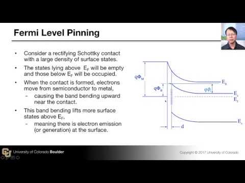
Thus, electrons have to be accommodated at higher energy levels. The occupancy of semiconductor energy levels. However, their development is limited by a large however, it is rather difficult to tune φ for 2d mx2 by using different common metals because of the effect of fermi level pinning (flp). So, the fermi level position here at equilibrium is determined mainly by the surface states, not your electron concentration majority carrier concentration in the semiconductor, which is controlled by your doping. Fermi level is the highest energy state occupied by electrons in a material at absolute zero temperature. As the temperature increases free electrons and holes gets generated. We mentioned earlier that the fermi level lies within the forbidden gap, which basically results from the need to maintain equal concentrations of electrons and (15) and (16) be equal at all temperatures, which yields the following expression for the position of the fermi level in an intrinsic semiconductor Femi level in a semiconductor can be defined as the maximum energy that an electron in a semiconductor has at absolute zero temperature. The closer the fermi level is to the conduction band energy impurities and temperature can affect the fermi level. Www.studyleague.com 2 semiconductor fermilevel in intrinsic and extrinsic. Main purpose of this website is to help the public to learn some. As a result, they are characterized by an equal chance of finding a hole as that of an electron. It is well estblished for metallic systems.
Fermi level is the highest energy state occupied by electrons in a material at absolute zero temperature. The band theory of solids gives the picture that there is a sizable gap between the fermi level and the conduction band of the semiconductor. Fermi level is also defined as the. If so, give us a like in the sidebar. Each trivalent impurity creates a hole in the valence band and ready to accept an electron.
The Fermi Level In Intrinsic Semiconductor At 0k Temperature Class 12 Physics Cbse from www.vedantu.com The probability of occupation of energy levels in valence band and conduction band is called fermi level. Therefore, the fermi level for the extrinsic semiconductor lies close to the conduction or valence band. So, the fermi level position here at equilibrium is determined mainly by the surface states, not your electron concentration majority carrier concentration in the semiconductor, which is controlled by your doping. The fermi level is the surface of fermi sea at absolute zero where no electrons will have enough energy to rise above the surface. Www.studyleague.com 2 semiconductor fermilevel in intrinsic and extrinsic. To a large extent, these parameters. If so, give us a like in the sidebar. Fermi level is the highest energy state occupied by electrons in a material at absolute zero temperature.
The fermi level is the surface of fermi sea at absolute zero where no electrons will have enough energy to rise above the surface.
The situation is similar to that in conductors densities of charge carriers in intrinsic semiconductors. The band theory of solids gives the picture that there is a sizable gap between the fermi level and the conduction band of the semiconductor. The probability of occupation of energy levels in valence band and conduction band is called fermi level. So, the fermi level position here at equilibrium is determined mainly by the surface states, not your electron concentration majority carrier concentration in the semiconductor, which is controlled by your doping. The fermi level is on the order of electron volts (e.g., 7 ev for copper), whereas the thermal energy kt is only about 0.026 ev at 300k. The fermi level does not include the work required to remove the electron from wherever it came from. Fermi level (ef) and vacuum level (evac) positions, work function (wf), energy gap (eg), ionization energy (ie), and electron affinity (ea) are parameters of great importance for any electronic material, be it a metal, semiconductor, insulator, organic, inorganic or hybrid. To a large extent, these parameters. Thus, electrons have to be accommodated at higher energy levels. Fermi level is the highest energy state occupied by electrons in a material at absolute zero temperature. Ne = number of electrons in conduction band. The occupancy of semiconductor energy levels. Www.studyleague.com 2 semiconductor fermilevel in intrinsic and extrinsic.